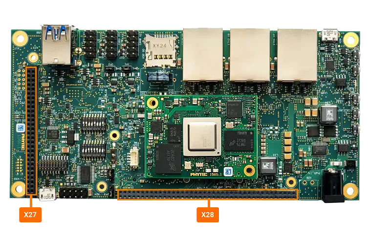
Expansion Connector
The phyCORE-AM64x development kit provides two expansion connectors, one at X27 60-pin (2x30-pin) and one at X28 80-pin (2x40-pin), both with 2mm pitch. These expansion connectors bring out signals that are available on the SOM connectors but were not used on the dev kit carrier board. Signals on the expansion connectors can be directly patched into by wires or used to mate a PHYTEC expansion board (or your own custom board). The pins at the connector can be freely multiplexed to enable different functionality at the expansion connector. To learn more information about the phyCORE-AM64x multiplexing, please refer to the Hardware Manual.
If you are designing a board to mate to one of the connectors, PHYTEC recommends the following:
Expansion Boards
These expansion board guides provide steps for evaluating the peripheral interfaces supported by the phyCORE-AM64x development kits expansion header.
Connector |
Description |
Mating Connector |
|---|---|---|
X27 |
60-pin (2x30-pin) 2mm |
Samtec TW-30-08-S-D-540-165 |
X28 |
80-pin (2x40-pin) 2mm |
Samtec TW-40-08-G-D-560-135 |
Note
Any 2mm pitch connector can be used to connect to sections of the expansion connectors.
The BSP has additional interface support through overlays that enable functions on the expansion connector. The signals that are available at the expansion connectors are listed below. The table includes a quick look of what PHYTEC has selected for common interfaces like I2C, SPI, and GPIO.
Pin Number |
Signal |
Description (lists default muxing) |
|---|---|---|
X27-1 |
VCC_3V3_SW |
3.3V Peripheral power rail |
X27-2 |
VCC_5V0_SW |
5.0V Peripheral power rail |
X27-3 |
VCC_1V8_EXP_CON |
1.8V Peripheral power rail |
X27-4 |
GND |
Ground |
X27-5 |
X_GPMC0_AD4/BM_4/FSI_RX3_D0/UART3_TX/GPIO0_82 |
UART3 Transmit Data. Connected to bootmode circuit. Routing depends on jumper setting. |
X27-6 |
X_GPMC0_AD5/BM_5/FSI_RX3_D1/UART3_nRTS/GPIO0_83 |
UART3 Request to Send. Connected to bootmode circuit. |
X27-7 |
X_GPMC0_AD9/BM_9/FSI_RX0_D0/UART3_nCTS/GPIO0_24 |
UART3 Clear to Send. Connected to bootmode circuit. Routing depends on jumper setting. |
X27-8 |
X_GPMC0_AD3/BM_3/FSI_RX3_CLK/UART3_RX/GPIO0_18 |
UART3 Receive Data. Connected to bootmode circuit. Routing depends on jumper setting. |
X27-9 |
GND |
Ground |
X27-10 |
X_PWR_EN |
PMIC power enable. Connected to reset circuit. |
X27-11 |
X_I2C1_SDA |
I2C1 Data. Used as I2C on CB. |
X27-12 |
X_ECAP0_IN_A/PWM_OUT/GPIO1_68 |
GPIO. Only connected to pin D16 on the SOM connector. |
X27-13 |
X_I2C1_SCL |
I2C1 Clock. Used as I2C on CB. |
X27-14 |
GND |
Ground |
X27-15 |
X_JTAG_TMS |
JTAG Test Mode Select Input. Connected to JTAG circuit. |
X27-16 |
X_JTAG_TRST |
JTAG Reset. By default X_nRESET_IN from the SOM is not connected to this pin. Not connected, routing depends on jumper setting. |
X27-17 |
X_JTAG_TDI |
JTAG Test Data Input. Connected to JTAG circuit. |
X27-18 |
X_JTAG_TDO |
JTAG Test Data Output. Connected to JTAG circuit. |
X27-19 |
GND |
Ground |
X27-20 |
X_JTAG_TCK |
JTAG Test Clock Input. Connected to JTAG circuit. |
X27-21 |
USB_HUB_DN4_D+ |
USB 4 High-speed differential transceiver (positive). Connected to USBHUB. |
X27-22 |
USB_HUB_DN4_D- |
USB 4 High-speed differential transceiver (negative). Connected to USBHUB. |
X27-23 |
X_PORz_OUT |
Cold Reset Status Output. Connected to reset. |
X27-24 |
GND |
Ground |
X27-25 |
X_UART0_CTS |
UART0 Clear to Send. Only connected to pin A7 on the SOM connector. |
X27-26 |
X_SPI1_CLK/EHRPWM6_SYNCI/GPIO1_49 |
SPI1 Clock. Only connected to pin D22 on the SOM connector. |
X27-27 |
X_UART0_RTS |
UART0 Request to Send. Only connected to pin A6 on the SOM connector. |
X27-28 |
X_SPI1_D0/GPIO1_50 |
SPI1 Data 0. Only connected to pin D19 on the SOM connector. |
X27-29 |
GND |
Ground |
X27-30 |
X_SPI1_D1/GPIO1_51 |
SPI1 Data 1. Only connected to pin D23 on the SOM connector. |
X27-31 |
X_GPMC0_AD3/BM_3/FSI_RX3_CLK/UART3_RX/GPIO0_18 |
UART3 Receive Data. Connected to bootmode circuit. Routing depends on jumper setting. |
X27-32 |
X_SPI1_CS0/GPIO1_47 |
SPI0 Chip Select 0. Only connected to pin D25 on the SOM connector. |
X27-33 |
X_GPMC0_AD4/BM_4/FSI_RX3_D0/UART3_TX/GPIO0_82 |
UART3 Transmit Data. Connected to bootmode circuit. Routing depends on jumper setting. |
X27-34 |
GND |
Ground |
X27-35 |
NC |
No connect |
X27-36 |
X_SPI1_CS1/I2C2_SDA/UART6_TX/GPIO1_48 |
SPI1 Chip Select 1. Only connected to pin D21 on the SOM connector. |
X27-37 |
USB_HUB_nPWRCTL4 |
USB Port 4 Power On Control. Connected to USBHUB. |
X27-38 |
REFCLK_DIST |
Clock distribution output. Connected to ETH Clock circuit. |
X27-39 |
USB_HUB_nOVERCUR4 |
USB Port 4 Overcurrent Detection. Connected to USBHUB. |
X27-40 |
X_EXTINTIN/RTC_nINT |
RTC Interrupt. Connected to RTC circuit. |
X27-41 |
GND |
Ground |
X27-42 |
X_ADC4 |
ADC Analog In 4. Only connected to pin D6 on the SOM connector. |
X27-43 |
X_ADC0 |
ADC Analog In 0. Only connected to pin D7 on the SOM connector. |
X27-44 |
X_ADC5 |
ADC Analog In 5. Only connected to pin D8 on the SOM connector. |
X27-45 |
X_ADC1 |
ADC Analog In 1. Only connected to pin D11 on the SOM connector. |
X27-46 |
GND |
Ground |
X27-47 |
X_ADC2 |
ADC Analog In 2. Only connected to pin D9 on the SOM connector. |
X27-48 |
X_ADC6 |
ADC Analog In 6. Only connected to pin D12 on the SOM connector. |
X27-49 |
X_ADC3 |
ADC Analog In 3. Only connected to pin D14 on the SOM connector. |
X27-50 |
X_ADC7 |
ADC Analog In 7. Only connected to pin D13 on the SOM connector. |
X27-51 |
GND |
Ground |
X27-52 |
X_MCU_SAFETY_ERRORn |
Error signal output from MCU Domain ESM. Only connected to pin D46 on the SOM connector. |
X27-53 |
X_RESET_REQz |
Warm Reset of MAIN Domain. Connected to reset circuit. |
X27-54 |
X_MCU_RESETSTATz |
MCU Domain Reset Status Output. Only connected to pin B7 on the SOM connector. |
X27-55 |
X_RESETSTATz |
MAIN Domain Reset Status Output. Connected to reset circuit. |
X27-56 |
GND |
Ground |
X27-57 |
VCC_IN |
12.0V input power rail |
X27-58 |
X_MCU_RESETz |
Warm Reset of MCU Domain. Connected to reset circuit. |
X27-59 |
NC |
No connect |
X27-60 |
VCC_5V0_MAIN |
5.0V Main SOM power rail |
X28-1 |
VCC_3V3_SW |
3.3V Peripheral power rail |
|---|---|---|
X28-2 |
VCC_5V0_SW |
5.0V Peripheral power rail |
X28-3 |
VCC_1V8_EXP_CON |
1.8V Peripheral power rail |
X28-4 |
GND |
Ground |
X28-5 |
X_PRG1_RGMII1_RD0 |
PRU RGMII Receive Data 0. Only connected to pin C52 on the SOM connector. |
X28-6 |
X_PRG1_RGMII1_RD1 |
PRU RGMII Receive Data 1. Only connected to pin C51 on the SOM connector. |
X28-7 |
X_PRG1_RGMII1_RD2 |
PRU RGMII Receive Data 2. Only connected to pin C49 on the SOM connector. |
X28-8 |
X_PRG1_RGMII1_RD3 |
PRU RGMII Receive Data 3. Only connected to pin C48 on the SOM connector. |
X28-9 |
GND |
Ground |
X28-10 |
X_PRG1_RGMII1_RXC |
PRU RGMII Receive Clock. Only connected to pin C57 on the SOM connector. |
X28-11 |
X_PRG1_RGMII1_RX_CTL |
PRU RGMII Receive Control. Only connected to pin C56 on the SOM connector. |
X28-12 |
X_PRG1_PRU0_GPO7/GPIO0_52 |
PRU GPIO. Only connected to pin c58 on the SOM connector. |
X28-13 |
X_PRG1_RGMII1_TD0 |
PRU RGMII Transmit Data 0. Only connected to pin C61 on the SOM connector. |
X28-14 |
GND |
Ground |
X28-15 |
X_PRG1_RGMII1_TD1 |
PRU RGMII Transmit Data 1. Only connected to pin C62 on the SOM connector. |
X28-16 |
X_PRG1_RGMII1_TD2 |
PRU RGMII Transmit Data 2. Only connected to pin C63 on the SOM connector. |
X28-17 |
X_PRG1_RGMII1_TD3 |
PRU RGMII Transmit Data 3. Only connected to pin C64 on the SOM connector. |
X28-18 |
X_PRG1_RGMII1_TX_CTL |
PRU RGMII Transmit Control. Only connected to pin C66 on the SOM connector. |
X28-19 |
GND |
Ground |
X28-20 |
X_PRG1_RGMII1_TXC |
PRU RGMII Transmit Clock. Only connected to pin C67 on the SOM connector. |
X28-21 |
X_PRG1_PRU0_GPO17/GPIO0_62 |
PRU GPIO. Only connected to pin C59 on the SOM connector. |
X28-22 |
X_PRG1_PRU1_GPO8 |
PRU GPIO. Only connected to pin B59 on the SOM connector. |
X28-23 |
X_PRG1_MDIO0_MDIO |
PRU MDIO Data. Only connected to pin C53 on the SOM connector. |
X28-24 |
GND |
Ground |
X28-25 |
X_PRG1_MDIO0_MDC |
PRU MDIO Clock. Only connected to pin C54 on the SOM connector. |
X28-26 |
X_CPSW_RGMII2_RD0 |
CPSW RGMII Receive Data 0. Only connected to pin C33 on the SOM connector. |
X28-27 |
X_CPSW_RGMII2_RD1 |
CPSW RGMII Receive Data 1. Only connected to pin C34 on the SOM connector. |
X28-28 |
X_CPSW_RGMII2_RD2 |
CPSW RGMII Receive Data 2. Only connected to pin C36 on the SOM connector. |
X28-29 |
GND |
Ground |
X28-30 |
X_CPSW_RGMII2_RD3 |
CPSW RGMII Receive Data 3. Only connected to pin C37 on the SOM connector. |
X28-31 |
X_CPSW_RGMII2_RX_CTL |
CPSW RGMII Receive Control. Only connected to pin C38 on the SOM connector. |
X28-32 |
X_CPSW_RGMII2_RXC |
CPSW RGMII Receive Clock. Only connected to pin C39 on the SOM connector. |
X28-33 |
X_CPSW_RGMII2_TD0 |
CPSW RGMII Transmit Data 0. Only connected to pin C41 on the SOM connector. |
X28-34 |
GND |
Ground |
X28-35 |
X_CPSW_RGMII2_TD1 |
CPSW RGMII Transmit Data 1. Only connected to pin C42 on the SOM connector. |
X28-36 |
X_CPSW_RGMII2_TD2 |
CPSW RGMII Transmit Data 2. Only connected to pin C43 on the SOM connector. |
X28-37 |
X_CPSW_RGMII2_TD3 |
CPSW RGMII Transmit Data 3. Only connected to pin C44 on the SOM connector. |
X28-38 |
X_CPSW_RGMII2_TX_CTL |
CPSW RGMII Transmit Control. Only connected to pin C46 on the SOM connector. |
X28-39 |
X_CPSW_RGMII2_TXC |
CPSW RGMII Transmit Clock. Only connected to pin C47 on the SOM connector. |
X28-40 |
X_CPSW_MDIO |
CPSW Management Data IO. Used in ETH0 circuit. |
X28-41 |
GND |
Ground |
X28-42 |
X_CPSW_MDC |
CPSW Management Data Clock. Used in ETH0 circuit. |
X28-43 |
X_PRG1_PRU0_GPO8 |
PRU GPIO. Only connected to pin B43 on the SOM connector. |
X28-44 |
X_PRG1_PRU0_GPO5 |
PRU GPIO. Only connected to pin B58 on the SOM connector. |
X28-45 |
X_PRG1_PRU1_GPO5 |
PRU GPIO. Only connected to pin B44 on the SOM connector. |
X28-46 |
GND |
Ground |
X28-47 |
X_GPMC0_CSn3/I2C2_SDA/GPIO0_44 |
GPIO. Only connected to pin C18 on the SOM connector. |
X28-48 |
X_GPMC0_CSn0/EQUEP0_S/GPIO0_41/PBC_nKILL |
GPIO. Used in PBC circuit. |
X28-49 |
X_GPMC0_CSn2/I2C2_SCL/GPIO0_43/PBC_nPFO |
GPIO. Used in PBC circuit. |
X28-50 |
X_GPMC0_CSn1/EQUEP0_I/GPIO0_42/PBC_nINT |
GPIO. Used in PBC circuit. |
X28-51 |
GND |
Ground |
X28-52 |
X_GPMC0_ADVn_ALE/FSI_RX5_CLK/UART5_RX/GPIO0_32/CAN0_nEN |
GPIO. Connected to CAN circuit. |
X28-53 |
X_GPMC0_CLK/FSI_RX4_CLK/UART4_nRTS/GPIO0_31 |
GPIO. Only connected to pin D4 on the SOM connector. |
X28-54 |
X_GPMC0_BE0n_CLE/FSI_TX1_D0/UART6_nRTS/GPIO0_35/CAN1_nEN |
GPIO. Connected to CAN circuit. |
X28-55 |
X_PORz_OUT |
Main Domain POR status output. Used in reset circuit. |
X28-56 |
GND |
Ground |
X28-57 |
X_nRESET_IN |
Cold system Reset. Used in reset circuit. |
X28-58 |
X_MCU_I2C1_SCL/MCU_GPIO0_20 |
MCU I2C1 Clock. Connected to light sensor circuit. |
X28-59 |
X_MCU_I2C1_SDA/MCU_GPIO0_21 |
MCU I2C1 Data. Connected to light sensor circuit. |
X28-60 |
X_MCU_SPI1_CLK/MCU_GPIO0_7 |
MCU SPI1 Clock. Connected to EEPROM circuit. |
X28-61 |
X_MCU_SPI1_D0/MCU_GPIO0_8 |
MCU SPI1 Data 0. Connected to EEPROM circuit. |
X28-62 |
X_MCU_SPI1_D1/MCU_GPIO0_9 |
MCU SPI1 Data 1. Connected to EEPROM circuit. |
X28-63 |
GND |
Ground |
X28-64 |
X_MCU_SPI0_CLK/MCU_GPIO0_11 |
MCU SPI0 Clock. Connected to EEPROM circuit. |
X28-65 |
X_MCU_SPI1_CS0/MCU_GPIO0_5 |
MCU SPI1 Chip Select 0. Connected to EEPROM circuit. |
X28-66 |
GND |
Ground |
X28-67 |
X_MCU_SPI0_D0/MCU_GPIO0_10 |
MCU SPI0 Data 0. Connected to EEPROM circuit. |
X28-68 |
X_MCU_SPI0_D1/MCU_GPIO04 |
MCU SPI0 Data 1. Connected to EEPROM circuit. |
X28-69 |
X_MCU_SPI0_CS0/MCU_GPIO0_13 |
MCU SPI0 Chip Select 0. Connected to EEPROM circuit. |
X28-70 |
X_MCU_SPI0_CS1/MCU_GPIO0_12 |
MCU SPI0 Chip Select 1. Only connected to pin D48 on the SOM connector. |
X28-71 |
X_MCU_UART1_nCTS/MCU_GPIO0_16 |
MCU_UART1 Clear to Send. Only connected to pin B28 on the SOM connector. |
X28-72 |
X_MCU_UART1_nRTS/MCU_GPIO0_17 |
MCU_UART1 Request to Send. Only connected to pin B25 on the SOM connector. |
X28-73 |
GND |
Ground |
X28-74 |
X_MCU_UART1_TX/MCU_GPIO0_15 |
MCU_UART1 Transmit Data. Only connected to pin B27 on the SOM connector. |
X28-75 |
X_MCU_UART1_RX/MCU_GPIO0_14 |
MCU_UART1 Receive Data. Only connected to pin B26 on the SOM connector. |
X28-76 |
GND |
Ground |
X28-77 |
X_MCU_UART0_nRTS |
MCU_UART0 Request to Send. Only connected to pin B56 on the SOM connector. |
X28-78 |
X_MCU_UART0_nCTS |
MCU_UART0 Clear to Send. Only connected to pin B57 on the SOM connector. |
X28-79 |
VCC_IN |
12.0V input power rail |
X28-80 |
VCC_5V0_MAIN |
5.0V Main SOM power rail |